
VLSI Design Flow
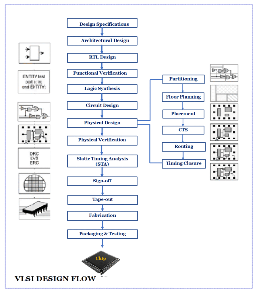
VLSI (Very-Large-Scale-Integration) design is the process of integrating millions or billions of transistors onto a single substrate. It describes the step-by-step procedure for converting a design specification into a chip layout (GDSII) ready for fabrication. It consists of a series of well-defined stages designed to ensure the chip’s operation, performance, and manufacturability. The flow diagram of VLSI design is shown here, along with a detailed explanation of each design stage.
The flow is divided into: 1. Front-End Design (Logical) 2. Back-End Design (Physical).
- Design Specifications: Design Specification is the first and most important stage in the VLSI design flow. It defines what the chip is supposed to do before any architecture or RTL design begins. A complete specification document typically includes:
- Functionality Requirements: What operations the chip must perform.
- Performance Requirements: Speed/ Throughput, Latency, lock Speed.
- Power Requirements: Power budget, Active and standby power targets.
- Area / Cost Requirements: Die size constraints, Packaging (BGA/QFN/3D IC/Chiplet). Ex: Die must not exceed 80 mm²
- Technology / Foundry Node: 7nm, 14nm, 28nm, 45nm, 65nm etc.
- Memory & I/O Requirements: SRAM size, cache architecture, memory bandwidth, Number of external I/O pins and interface types. This becomes the benchmark for the rest of the design.
- Architecture Design: Architecture Design is the second stage in the VLSI design flow, after System Specification. If System Specification defines what the chip should do, then Architecture Design defines how the chip will do it. It converts the high-level product requirements into a technical design plan for the chip. At this stage, the designer has to decide the internal structure of the chip so that all specification goals (performance, power, area, functionality) are met. Accordingly, splits the complete system into blocks / modules and defines: What each block will do, How the blocks interact, How data flows inside the chip. Architecture Design defines modules, datapath, control path, pipeline depth, memory organization, communication interfaces, and power management strategy. The result is the micro-architecture document that guides RTL design.
- RTL Design: RTL Design (Register Transfer Level Design) is the third stage in the VLSI design flow. After the Architecture Design defines how the chip should work, RTL Design converts that architecture into code using HDLs (Hardware Description Languages) such as:
- VHDL
- Verilog HDL
- System Verilog This RTL code describes how data flows between registers and how combinational logic transforms the data on every clock cycle.
- Goals of RTL Design:
- Implement the architecture specifications accurately
- Write synthesizable code
- Ensure functionality, timing, and reset behavior are modeled correctly
- Maintain readability and reusability of code
- The main output of RTL design is a directory containing
.vhd /.v / .svfiles for the entire chip. - If RTL design has mistakes:
- Verification will fail
- Synthesis will generate incorrect hardware
- Silicon will fail → costly re-spin
- So RTL must be:
- Functionally correct
- Synthesizable
- Timing-aware
- Modular & readable
- Functional Verification: Functional Verification is the fourth stage in the VLSI design flow, after RTL Design. It ensures that the RTL design works exactly according to the specification and architecture, with no functional bugs.
- Functional Verification checks “Did we design the chip right?”
- About 70% of VLSI design time is spent on verification because catching bugs before fabrication is critical.
- Functional Verification is to prove that:
- RTL logic = expected functionality
- All corner cases are handled
- No unintended behavior exists
- Logic Synthesis: Logic Synthesis is the fifth stage in the VLSI design flow, after Functional Verification. It converts RTL code (Verilog/VHDL/System Verilog) into a Gate-Level Netlist using standard cells from a technology library. Logic Synthesis converts behavioral RTL into actual digital hardware (gates + flip-flops) that can be physically implemented on silicon. Netlist contains logic gates such as AND, OR, XOR, MUX, FF, etc., connected based on RTL functionality.
- Synthesis tool perform the following operations
- 1. Parse & Elaborate RTL: Reads RTL, resolves hierarchy, parameters, constants.
- 2. Mapping to Standard Cells: Combinational logic → AND/OR/XOR/MUX gates. Sequential logic → D-Flip-Flops, scan FFs
- 3. Optimization for:
- Timing
- Area
- Power
- Tools restructure logic based on constraints.
- If synthesis is wrong:
- Timing failures during Physical Design
- More power consumption
- Larger area → higher cost
- Silicon malfunction
- So synthesis ensures that:
- RTL is converted to gates
- Meets timing/power/area targets
- Ready for Physical Design
- Circuit Design: Circuit design step appears only for custom blocks, like:
- Memory sense amplifier
- PLL/VCO
- Bandgap reference
- Level shifters
- IO pads
- Custom high-speed adders, multipliers
- This is called Custom Circuit Design / Transistor-level Design.
- Physical Design: Physical Design in VLSI Design can be done in a sequence of 6 stages. Those stages are:
- 1.Partitioning
- 2. Floorplanning
- 3. Placement
- 4. Clock Tree Synthesis
- 5. Routing
- 6. Timing Closure
- 7.1 Partitioning: Modern VLSI chips may contain millions to billions of transistors. Designing them as a single block is impossible. So, the system is partitioned into sub-blocks. Partitioning refers to dividing a large design into smaller manageable blocks (modules) so it can be implemented efficiently in terms of area, performance, power, routing, and reusability.
- 7.2 Floorplanning: Floorplanning is the first major step in the Physical Design (Backend) flow, after synthesis. It determines the physical arrangement of major blocks on the chip just like designing the layout of rooms in a house before construction begins. Floorplanning decides where each module (macros, memory, IPs, logic) will be placed on silicon to achieve optimal performance, power and area.
- A good floorplan must:
- Minimize routing congestion
- Meet timing across the chip
- Minimize power and IR drop
- Use the area efficiently
- Allow easy clock distribution and power delivery
- 7.3 Placement: Placement is the stage in Physical Design where all standard cells (logic gates, flops, buffers, etc.) are placed in the chip core at legal locations without overlap. The netlist is mapped to physical locations, but routing is not done yet — only the positions of cells are finalized to optimize:
- Timing
- Area
- Power
- Routing congestion
- Placement decides where each standard cell will sit on silicon so that timing and routing later become easier.
- 7.4 Clock Tree Synthesis (CTS): Clock Tree Synthesis is the stage in Physical Design where the clock signal is distributed to all sequential elements (flip-flops, latches) in the chip with minimal skew and latency.
- Before CTS, the design has:
- Placed standard cells
- No clock buffers or clock routing
- After CTS:
- Clock buffers / inverters are inserted
- A balanced clock network is built
- CTS builds the physical clock network so that the clock reaches all flip-flops at almost the same time.
- Before CTS, the design has:
- 7.5 Routing: Routing is the stage in Physical Design where electrical connections (wires) are made between all placed cells, macros, and I/O pins using metal layers on the chip.
- Before routing:
- Cells are placed, but their pins are not connected with wires
- After routing:
- All nets (signals, clock, reset, scan, power) are physically connected
- Routing draws the “roads” (wires) on the chip so that signals can travel from one cell to another exactly as defined in the netlist.
- Before routing:
- 7.6 Timing closure: Timing closure means ensuring that all timing paths in the chip meet the required timing constraints after physical implementation (placement, CTS, routing, etc.).
In simple words:
Timing closure = Making sure the chip works at the target clock frequency without timing violations.
- Physical Verification: Physical Verification (PV) is the stage in VLSI design where the final routed layout is checked for manufacturing correctness before sending the chip to the foundry. Even if a design works functionally, it cannot be fabricated unless it passes physical verification. Physical Verification ensures the layout is correct, manufacturable, and matches the circuit connectivity.
- During manufacturing, if layout rules are violated:
- Chip may short circuit
- Chip may break open
- Chip may fail timing
- Yield may drop drastically
- So PV guarantees the layout is clean, correct, and safe to fabricate.
- Types of Physical Verification:
- DRC — Design Rule Check
- Checks whether layout obeys foundry rules:
Minimum metal width
Minimum spacing
Via requirements
End-of-line spacing
Notch/overlap rules
Antenna rules - If the design has DRC errors, layout cannot be fabricated.
- Checks whether layout obeys foundry rules:
- LVS — Layout vs Schematic
- Ensures that the layout connectivity matches the netlist.
It checks:
Are the correct transistors present?
Are they connected to the correct nodes?
Are short/open errors present? - LVS mismatch → chip logic becomes wrong.
- Antenna Check
During fabrication, long metal wires can accumulate charge and damage gate oxides.
Antenna check ensures:
Protection diodes/breaks are added where needed - ERC — Electrical Rule Check
Checks for electrical reliability issues such as:
Floating pins
Unconnected inputs
Power/Ground shorts
Mixed-signal isolation issues. - DFM — Design for Manufacturability Checks
Optional but recommended for high-yield chips:
Metal density fill
Lithography hotspots
CMP (chemical polishing) defects.
- Ensures that the layout connectivity matches the netlist.
- DRC — Design Rule Check
- During manufacturing, if layout rules are violated:
- STA (Static Timing Analysis): Static Timing Analysis is the process of verifying that all timing paths in the chip meet setup and hold requirements without applying input vectors or simulation.
- STA checks timing mathematically over every possible path.
- STA ensures that signals reach flip-flops in time for correct data capture at every clock cycle.
- Why STA is needed?
Even if functionality is correct, a chip can fail due to timing errors.
STA ensures:
Chip runs at intended frequency
No setup or hold violations
Timing safety across PVT corners (Process, Voltage, Temperature)
It checks billions of timing paths — something simulation cannot do.
- Sign-off: Sign-off is the final series of checks performed on a fully completed design to confirm that it is safe for fabrication.
- Sign-off guarantees the design is functionally correct, timing clean, power safe, and physically manufacturable.
- If any sign-off check fails → the chip cannot go for tape-out.
- Sign-off ensure that the chip will:
- Work correctly in silicon
- Meet performance and power targets
- Be manufacturable without risk
- Have high yield and long-term reliability
- Major Types of Sign-off:
1. Timing Sign-off
Uses STA (Static Timing Analysis)
Includes multi-corner, multi-mode (MCMM) timing closure
Considers extracted parasitics (SPEF/QRC)
Goal → No setup/hold violations in all corners.
2. Power Sign-off
Ensures power delivery and consumption are within limits:
IR-drop analysis
Electromigration (EM) analysis
Thermal analysis
Switching activity based power checks
Goal → No IR-drop or EM failures; power within spec
3. Physical Verification Sign-off
Includes:
DRC (Design Rule Check)
LVS (Layout vs Schematic)
Antenna checks
ERC (Electrical Rule Check)
Goal → Manufacturing rule compliance
4. Signal Integrity (SI) Sign-off
Verifies:
Crosstalk delay
Crosstalk noise
Coupling capacitance issues
Goal → No data corruption due to noise
5. Reliability Sign-off
Checks long-term safety:
NBTI / PBTI aging
Hot carrier injection (HCI)
Electrostatic discharge (ESD)
Goal → Chip remains safe over lifetime.
- Tape-out: Tape-out is the final stage of the VLSI design flow, where the completed chip design is sent to the semiconductor fabrication (foundry) for manufacturing.
- GDSII (Graphic Data System II) is the final layout file format sent to the semiconductor foundry for chip fabrication.
- After Sign-off, all layout data (cells, routing, layers, masks) is merged and exported into a single GDSII file.
- GDSII Generation converts the complete layout database into a single manufacturing-ready file used to create photomasks for wafer fabrication.
Tape-out = delivery of GDSII to foundry.
- Fabrication: Fabrication is the process of physically creating the integrated circuit (IC) on a silicon wafer using the GDSII layout file provided by the design team. Fabrication happens in a cleanroom semiconductor foundry (e.g., TSMC, Intel, Samsung, GlobalFoundries).
- Fabrication converts the design (GDSII) into real hardware (silicon chip) using advanced chemical, optical, and material processes.
- Billions of transistors, interconnects, vias, and metal layers are built layer-by-layer on the silicon wafer.
- Modern chips (7nm / 5nm / 3nm):
Contain >50 metal layers
Have >100 billion transistors
Require ~1000+ manufacturing steps - Fabrication happens in Class 1 – Class 100 cleanrooms, where: Air is 99.999% filtered, Temperature and humidity are precisely controlled, Workers wear bunny suits Because a single dust particle can destroy the device.
- Packaging and Testing:
After fabrication, chips exist as tiny dies on a silicon wafer, but cannot be used directly.
Packaging and Testing transform the fabricated die into a usable, reliable, and protected electronic component.- Packaging protects the chip and enables external electrical connections.
- Testing ensures only good chips are shipped, and faulty ones are rejected.
- Packaging provides:
- Electrical connections to PCB
- Protection from environment
- Mechanical support
- Heat dissipation path
- Final Testing (after packaging) is performed after packaging to ensure:
- Timing performance
- Interface functionality
- Thermal stability
- Reliability & stress tests
- After testing the Passed chips will be shipped to customers and the failed chips will be marked as defective or downgraded (binning).
Chip Binning (Important industry concept)
Chips from the same wafer do not have identical performance.
Example:
Highest-performing parts → flagship model
Medium performance → mid-range
Low performance → budget model
This is why CPUs/GPUs come in multiple models even though they are manufactured together.
🌟 The Full VLSI Journey (one line)
RTL → Netlist → Layout → GDSII → Fabrication → Packaging → Testing → Final IC
I really value your work, Great post.